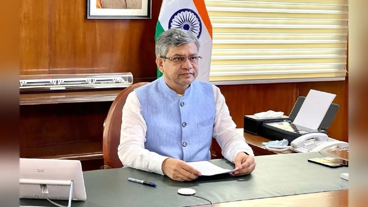
The Union Cabinet chaired by Prime Minister Narendra Modi approved India Semiconductor Mission 2.0 (ISM 2.0) or Semicon 2.0 project on July 15, 2026 at a cost of ₹1.27 lakh crore. Speaking to the media about this decision, Union Minister Ashwini Vaishnaw informed that the semiconductor industry is a fundamental industry wherein you find chips in everything such as mobiles, fridge, cars, train, home appliances, and so forth.
This approval comes after seven other cabinet approvals that were undertaken on the same day, having an outlay of ₹2.19 lakh crore in addition to the mobile phone manufacturing scheme, urea self-reliance policy, and railway infrastructure.
While there may be no other structural change in ISM 2.0 besides the increase in amount, it is worth mentioning that the government has extended the time span during which it operates from five years to twelve years. This was done on purpose in order to encourage long-term institutional investors who would like to invest in such capital-intensive industries as fabs, testing units, and assembly lines. It takes years for those investments to become profitable.
And extending the lifespan of the scheme indicates to investors in the semiconductor business that India will stick to its plan in the long term.
This also means that ISM 2.0 is philosophically different from the first phase of the program.
The initial launch of ISM was initiated with the amount of ₹76,000 crore allocation after Cabinet approval in December 2021, and it was all about proving to the world that India can manufacture chips at all. At that stage, India was just setting up the facilities needed for Assembly, Testing, Marking, and Packaging (ATMP).
As per the government, the new mission is built on six pillars that cover all aspects of the semiconductor industry:
- Chip design—This pillar focuses on developing the design ecosystem further by helping create IP, chip designs, and semiconductor systems for defense and commercial purposes, as there are about 105 start-ups already working on chip design in India.
- Equipment, materials, and supply chain — The government plans to reward those businesses which manufacture semiconductor equipment, chemicals, gases, and materials that are required for chip manufacturing, as there has always been a gap in the supply chain through which India used to import even for its basic manufacturing needs.
- Fab capacity—As the first semiconductor fab of India will be operational from 2028, this pillar tries to attract investments in silicon fabs, compound semiconductor fabs, discrete fabs, and display fabs.
- Enhancement of ATMP and OSAT – Following from the previous ISM initiative which promoted packaging technology, this pillar is geared towards bringing in advanced ATMP and Outsourced Semiconductor Assembly and Test (OSAT) technologies due to increased interest by global companies to manufacture in India other than current manufacturing centers.
- Research and Development – At present, manufacturing of semiconductor chips in India occurs at 28 nm to 110 nm technology nodes; this pillar is geared towards developing more advanced technology nodes through collaborations between research institutes both within and outside India.
- Talent development – With around 315 universities providing education to students using industry standard Electronic Design Automation (EDA) tools and 68,000 students so far trained, this pillar is geared towards developing a skilled labor force needed for a developed semiconductor chip industry.
It becomes easier to gauge the extent of ISM 2.0 when considering what ISM 1.0 achieved. Under the first phase, the Government approved 12 semiconductor manufacturing and packaging projects, which attracted an investment of over ₹1.64 lakh crore – well above twice the total investment made under the scheme itself. This list comprises the first ever chip factory project of India – a joint venture between Tata Group and Taiwan’s Powerchip Semiconductor Manufacturing Corporation, estimated at nearly ₹91,000 crore, along with silicon carbide fabs, gallium nitride micro LED display fabs, and 9 packaging factories catering to industries ranging from consumer electronics and automobiles to telecommunications and aerospace industry segments.
The first ISM project to be approved was Micron’s assembly, test, marking, and packaging facility in Sanand, Gujarat, that received approval in June 2023. Of the total 12 projects approved under the scheme, three have already started their operations, while those from Sanand have apparently been earmarked for exports to countries including Japan, the United States, and Europe.
It is expected that the implementation of ISM 2.0 will draw an additional investment of around ₹4 lakh crore and will enable the manufacture of semiconductors valued at ₹2 lakh crore. It should also be noted that the mission comes at a time when global supplies of memory chips are facing pressure, thus providing India another chance to develop its semiconductor capabilities as manufacturers seek to spread out their production beyond the concentrated production facilities of East Asia. In this regard, Vaishnaw said that the country hopes to be self-sufficient in terms of production of chips by the end of the program.
Besides ISM 2.0, the Cabinet also approved the Phase II of Mobile Phone Manufacturing Scheme worth ₹62,500 crore, further highlighting the idea that semiconductor policy and electronics manufacturing policy have come to align with one another, chips directly going into making phones and other electronics and automobiles.
For a nation that has been importing the majority of its chips for decades now, ISM 2.0 is both an intention and a financing strategy.
Semiconductors have been seen by the world to represent the convergence of economics, security, and sovereignty. An advanced fabrication facility could anchor a whole regional ecosystem of suppliers of components and equipment along with highly skilled engineers. By extending the timeline to twelve years for this programme, the government seems to have recognised one harsh reality of the industry, which is chip fabs are neither constructed nor do they become profitable in an electoral timeframe.
Meanwhile, the ambition brings execution risks of its own. It is expected that the first fab in the country would come up only by 2028, while the transition from mature process nodes such as 110nm to advanced process nodes would require continuous R&D expenditure and cooperation with international research facilities in which India is lagging behind. Additionally, talent is expected to expand significantly beyond the current numbers of 68,000 students trained so far.